The official website - Shenzhen Mingjiada Electronic Co., LTD

H9CKNNNBKTMTDR high-speed synchronous DRAM device internally configured as an 8-bank memory
Features
[ FBGA ]
Operation Temperature
- -30'C ~ 105'C
Packcage
- 216-ball FBGA
- 15.0x15.0mm2, 0.70t, 0.50mm pitch
- Lead & Halogen Free
[ LPDDR3 ]
VDD1 = 1.8V (1.7V to 1.95V)
VDD2, VDDCA and VDDQ = 1.2V (1.14V to 1.30)
HSUL_12 interface (High Speed Unterminated Logic 1.2V)
Double data rate architecture for command, address and data Bus;
- all control and address except CS_n, CKE latched at both rising and falling edge of the clock
- CS_n, CKE latched at rising edge of the clock
- two data accesses per clock cycle
Differential clock inputs (CK_t, CK_c)
Bi-directional differential data strobe (DQS_t, DQS_c)
- Source synchronous data transaction aligned to bi-directional differential data strobe (DQS_t, DQS_c)
- Data outputs aligned to the edge of the data strobe (DQS_t, DQS_c) when READ operation
- Data inputs aligned to the center of the data strobe (DQS_t, DQS_c) when WRITE operation
DM masks write data at the both rising and falling edge of the data strobe
Programmable RL (Read Latency) and WL (Write Latency)
Programmable burst length: 8
Auto refresh and self refresh supported
All bank auto refresh and per bank auto refresh supported
Auto TCSR (Temperature Compensated Self Refresh)
PASR (Partial Array Self Refresh) by Bank Mask and Segment Mask
DS (Drive Strength)
DPD (Deep Power Down)
ZQ (Calibration)
ODT (On Die Termination)
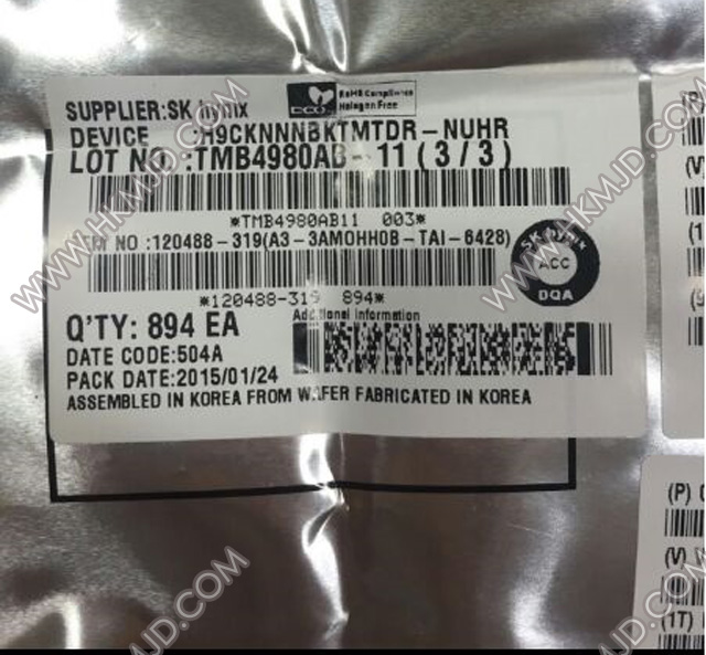
Picture:
MJD is a corporation which engaged in agency electronic components. MJD Through seventeen years unrimitting efforts, aspire to provide our customers with world-leading products and service. Nowalready became a one of the most famous electronic components distributor in China.
Shen Zhen Mingjiada electronic.Co.,ltd.