The official website - Shenzhen Mingjiada Electronic Co., LTD

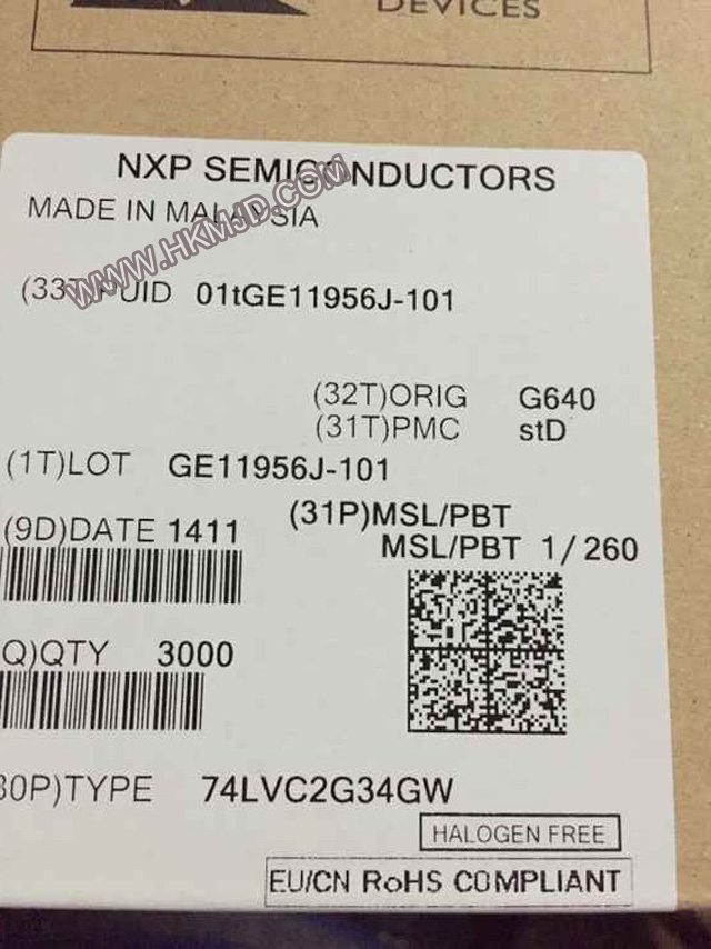
74LVC2G34GW Dual buffer gate
|
|
||
|
Dual buffer gate |
||
|
Application |
partial power-down applications |
|
|
Description |
Wide supply voltage range from 1.65 V to 5.5 V 5 V tolerant inputs for interfacing with 5 V logic High noise immunity Complies with JEDEC standard: JESD8-7 (1.65 V to 1.95 V) JESD8-5 (2.3 V to 2.7 V) JESD8B/JESD36 (2.7 V to 3.6 V) ESD protection: HBM JESD22-A114F exceeds 2000 V MM JESD22-A115-A exceeds 200 V 24 mA output drive (VCC = 3.0 V) CMOS low power consumption Latch-up performance exceeds 250 mA Direct interface with TTL levels Multiple package options Specified from 40C to +85C and 40C to +125C. |
|
|
Want know more us? Please check out www.mjdic.com/ |
||