The official website - Shenzhen Mingjiada Electronic Co., LTD

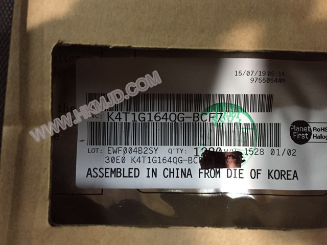
K4T1G164QG-BCF7 1Gb G-die DDR2 SDRAM
|
|
||
|
1Gb G-die DDR2 SDRAM |
||
|
Application |
general applications. |
|
|
Description |
Speed DDR2-667 5-5-5 DDR2-800 6-6-6 DDR2-800 5-5-5 DDR2-1066 7-7-7 Units 7CAS Latency 5 6 5 7 tCK tRCD(min) 15 15 12.5 13.125 ns tRP(min) 15 15 12.5 13.125 ns tRC(min) 60 60 57.5 58.125 ns JEDEC standard VDD = 1.8V ± 0.1V Power Supply • VDDQ = 1.8V ± 0.1V • 333MHz fCK for 667Mb/sec/pin, 400MHz fCK for 800Mb/sec/pin, 533MHz fCK for 1066Mb/sec/pin • 8 Banks • Posted CAS • Programmable CAS Latency: 3, 4, 5, 6, 7 • Programmable Additive Latenc y: 0, 1, 2, 3, 4, 5, 6 • Write Latency(WL) = Read Latency(RL) -1 • Burst Length: 4 , 8(Interleave/nibble sequential) • Programmable Sequential / Interleave Burst Mode • Bi-directional Differential Data-Strobe (Single-ended data-strobe is an optional feature) • Off-Chip Driver(OCD) Impedance Adjustment • On Die Termination • Special Function Support - 50ohm ODT - High Temperature Self-Refresh rate enable • Average Refresh Period 7.8us at lower than TCASE 85C, 3.9us at 85C < TCASE < 95 C • All of products are Lead-Free, Halogen-Free, and RoHS compliant |
|
|
Want know more us? Please check out www.mjdic.com/ |
||