TI ADC12D040CIVS Dual-Channel 12-Bit 40MSPS 600mW ADC With Internal/External Reference
Shenzhen Mingjiada Electronics Co., Ltd., as a leading global distributor of electronic components, has been supplying TI's original
ADC12D040CIVS analogue-to-digital converter (ADC) for an extended period. This high-performance 12-bit dual-channel 40 MSPS ADC, with its excellent dynamic performance, low-power design, and stable reliability, is widely used in communication equipment, test instruments, medical imaging, and industrial automation fields.
The ADC12D040CIVS is a dual-channel, low-power single-chip CMOS analogue-to-digital converter capable of converting analogue input signals into 12-bit digital values at a rate of 40 million samples per second (Msps). The converter employs a differential pipeline architecture, featuring digital error correction functionality and on-chip sampling hold circuits, enabling exceptional dynamic performance while minimising chip area and power consumption. Operating on a single 5V power supply, the ADC12D040CIVS achieves 10.9 effective bits at a 10 MHz input and consumes only 600 mW of power at 40 Msps (including reference current). The power-down feature reduces power consumption to 75 mW.
Differential inputs provide a full-scale differential input swing equal to 2VREF, while also supporting single-ended inputs. It is recommended to fully utilise differential inputs for optimal performance. The digital outputs of the two ADCs are provided via independent 12-bit buses, with the output data format selectable between offset binary or two's complement format.
To facilitate interface connections, the digital output drive power supply pins of the
ADC12D040CIVS can be connected to an independent supply voltage (range: 2.4 V to the digital supply voltage), enabling compatibility with low-voltage systems. The ADC12D040CIVS's speed, resolution, and single-supply operation characteristics make it suitable for a wide range of applications.
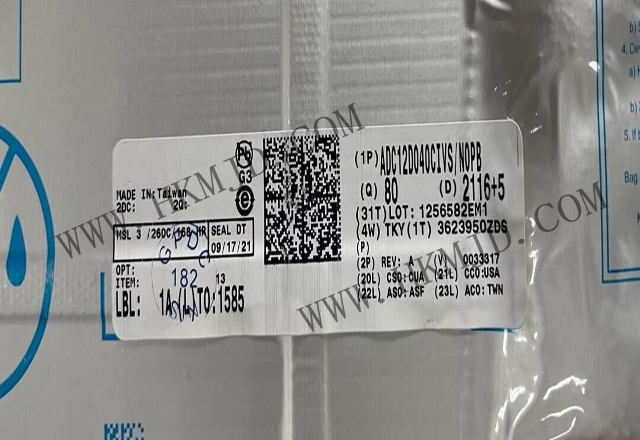
The
ADC12D040CIVS is housed in a 64-pin TQFP package and operates within the industrial temperature range of -40°C to +85°C. An evaluation board is available to simplify the product evaluation process.
Resolution: 12 bits
Number of channels: 2 channels
Interface type: Parallel
Sampling rate: 40 MS/s
Input type: Differential
Architecture: Pipeline
Analogue supply voltage: 4.75 V to 5.25 V
Digital supply voltage: 2.35 V to 5.25 V
Signal-to-noise ratio (SNR): 69 dB
Minimum operating temperature: -40°C
Maximum operating temperature: +85°C
Differential non-linearity (DNL): ±0.4 LSB
Effective number of bits (ENOB): 10.9 bits
Features: Low power consumption
Gain error: -2.7% FSR to +4% FSR
INL - Integral non-linearity: 2 LSB
Input voltage: 4 V
ADC input channels: 2 channels
Number of converters: 2 converters
Operating supply voltage: 5 V
Power consumption: 600 mW
As a high-performance analogue-to-digital converter, ADC12D040CIVS integrates multiple advanced technologies and demonstrates outstanding performance metrics in signal acquisition systems. This dual-channel ADC adopts a pipeline architecture, achieving a perfect balance between high-speed sampling and high-precision conversion, making it particularly suitable for complex application scenarios requiring synchronous acquisition of multiple signals.
Core Performance Parameters:
The core performance metrics of the
ADC12D040CIVS highlight its leading position in the 12-bit ADC category:
Resolution and Sampling Rate: Offers 12-bit resolution and a conversion rate of 40 MSPS (40 million samples per second), enabling precise capture of rapidly changing analogue signals and meeting broadband signal processing requirements.
Input Configuration: Supports differential input mode to effectively suppress common-mode noise and enhance signal integrity. Each channel has an independent analogue input pin for convenient system design.
Dynamic Performance: At a 40 MSPS sampling rate, the typical signal-to-noise ratio (SNR) reaches 70 dB, and the spurious-free dynamic range (SFDR) is 85 dB, ensuring high-quality signal acquisition.
Power consumption performance: Typical power consumption is only 600mW, offering a significant energy efficiency advantage over comparable products, helping to reduce overall system power consumption
Power requirements: The analogue section is powered by a single 5V supply, while the digital section supports a wide voltage range from 2.35V to 5.25V, providing design flexibility
Architecture and interface features:
The internal architecture and interface design of the
ADC12D040CIVS are fully tailored to the practical requirements of high-speed data acquisition systems:
Pipeline conversion architecture: Utilises a multi-stage pipeline structure to maintain high conversion rates while ensuring accuracy, with an integrated sampling and holding (S/H) circuit, achieving a conversion ratio of 1:13
Parallel Data Interface: Provides a standard parallel data output interface for direct connection to an FPGA or DSP, simplifying system design and reducing latency
Reference Voltage Selection: Supports both internal and external reference voltage modes, allowing users to flexibly configure based on system accuracy requirements. The internal reference voltage simplifies design, while the external reference provides a higher precision option
Clock Input: Features a single-ended clock input design supporting a wide range of clock frequencies, facilitating synchronization with various system clocks
ADC12D040CIVS demonstrates exceptional application value in numerous fields requiring high-speed data acquisition, thanks to its dual-channel synchronous sampling, 40 MSPS high conversion rate, and 12-bit resolution.
Communication Infrastructure Equipment
In modern communication systems, the
ADC12D040CIVS is an ideal choice for building high-performance receiver chains:
Base Station Transceiver Systems: Used for intermediate frequency sampling digitisation, supporting multi-carrier GSM, CDMA, and LTE signal processing. The dual-channel design facilitates synchronous acquisition of I/Q signals, simplifying the implementation of digital down-conversion (DDC).
Software-Defined Radio (SDR): Its high dynamic range and 40 MSPS sampling rate enable it to process wideband signals, meeting the dual requirements of flexibility and performance for SDR platforms.
Microwave Backhaul Equipment: Used for digitising modulated signals in point-to-point microwave communications, its excellent SFDR performance helps maintain signal quality
Medical imaging systems
In the medical electronics field, the high precision and low noise characteristics of the
ADC12D040CIVS make it the preferred choice for various imaging devices:
Ultrasound imaging systems: Used for digitising echo signals returned by transducers, the dual-channel design can simultaneously process multiple ultrasound signals, improving imaging frame rates
Digital X-ray detectors: Used for photodiode signal acquisition in flat-panel detectors, the 12-bit resolution is sufficient to distinguish subtle density differences
Optical coherence tomography (OCT): The high-speed sampling capability meets the axial scanning rate requirements of OCT systems, supporting high-resolution imaging of biological tissues
Industrial Automation and Test Measurement
Industrial environments impose stringent requirements on data acquisition equipment for high reliability and interference resistance. The ADC12D040CIVS is fully capable of meeting these demands:
High-speed data acquisition systems: Used in applications such as vibration analysis and acoustic testing that require capturing transient signals, the 40 MSPS sampling rate accurately records rapidly changing physical quantities
Automated Test Equipment (ATE): In multi-parameter synchronous testing, the dual-channel ADC reduces the number of components and simplifies the system architecture
Power Quality Analyser: Simultaneously captures multi-phase voltage and current signals, analyses harmonics and transient phenomena, and the differential input effectively suppresses common-mode noise in industrial environments
Defence and Aerospace Systems
In the demanding defence and aerospace sectors, the
ADC12D040CIVS demonstrates outstanding environmental adaptability:
Radar Signal Processing: Used for digitising intermediate frequency signals, its wide temperature range (-40°C to 85°C) adapts to various operating environments.
Electronic warfare systems: High-speed sampling capability meets the demand for capturing transient signals, supporting spectrum monitoring and signal analysis
Flight data recording: Simultaneous acquisition of multiple parameters of aircraft status information, with industrial-grade reliability ensuring data integrity
If you are interested, please contact Mr. Chen:
QQ: 1668527835
Tel: 13410018555
Email: chen13410018555@163.com