The official website - Shenzhen Mingjiada Electronic Co., LTD

The 9FGV0841AKLF is an ultra-low power clock generator from Renesas, which is mainly used in the field of PCI Express (PCIe) and other high-speed communication interfaces. The following are its core parameters:
Product type: Clock Generators
Number of Output terminals: 8 Output
Maximum output frequency: 100 MHz
Maximum input frequency: 27 MHz
Packaging/Cabinet: VFQFPN-48
Beat: 250 ps
Power supply voltage - maximum: 1.9V
Power supply voltage - minimum: 1.7V
Series: 9FGV0841
Working power supply current: 35 mA
Minimum operating temperature: 0 ° C
Maximum operating temperature: + 70 ° C
Installation style: SMD/SMT
Packaging: Tray
Height: 0.9mm
Length: 6mm
Humidity sensitivity: Yes
Working power supply voltage: 1.7V to 1.9V
Width: 6mm
Part number alias: 9FGV0841
Unit weight: 1.324 g
Description
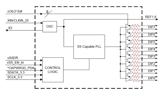
9FGV0841AKLF is a member of Renesas' SoC-friendly 1.8V ultra-low power PCIe clock series. It features an integrated output terminal, providing Zo = 100Ω for connection in the direction of a 100Ω transmission line. The 9FGV0841AKLF also features 8 output enables for clock management, 2 different spread spectrum levels and 2 optional SMBus addresses.
The 9FGV0841AKLF clock generator mainly has the following features:
Conforming to the PCIe GEN1-4 standard
The integrated terminal provides 100ω differential Zo: reducing the number of components and circuit board space
1.8V operating voltage: Reduces power consumption
The output can be powered by any voltage ranging from 1.05V to 1.8V: maximizing power savings
OE# pin: Supports DIF power management
LP-HCSL differential clock output: Reduces power consumption and circuit board space
Programmable slew rate for each output: allows tuning for various line lengths
Programmable output amplitude: Allows tuning for various application environments
The DIF output is blocked until the PLL is locked: a clean system starts
Optional 0%, -0.25% or -0.5% expansion on DIF output: Reduces EMI
External 25MHz crystal; Supports tight ppm, with a synthesis error of 0ppm
Configuration can be accomplished through the bundling pin: device control does not require an SMBus interface
3.3V compatible with SMBus interface supports traditional controllers
Space-saving 6 × 6mm 48-VFQFPN; The smallest circuit board space
Optional SMBus address: Multiple devices can easily share one SMBus network segment
Offer AEC-Q100 certified Grade 2 (-40°C to +105°C) version (wettable side wing package)
Typical applications
9FGV0841AKLF is specifically designed for PCIe Gen1/2/3/4/5/6 and is suitable for server, storage and high-performance computing scenarios. It can reduce system clock jitter and optimize signal integrity. Typical applications include:
▪ Generation of PCIe GEN1-4 clock for the adapter card
▪ Memory
▪ Network
▪ JBOD
▪ Communication
▪ Access point
Supply information
If you need to purchase the 9FGV0841AKLF clock generator, please visit the official website of mingjiada (www.mjdic.com) for inquiries.