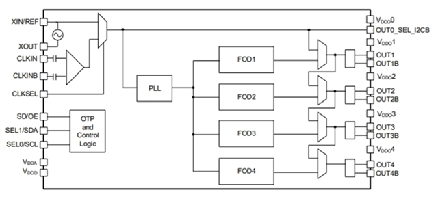

The 5P49V60B000NLG2 is a programmable clock generator used in automotive applications. The configuration can be stored in on-chip one-time programmable (OTP) memory or changed using the I2C interface. This is Renesas' sixth-generation programmable clock technology (VersaClock 6E). The following are its core features and functions:
Flexible 1.8V, 2.5V or 3.3V power rails
▪ High-performance, low phase noise PLL, output < 0.5ps RMS typical phase jitter
▪ Four sets of internal OTP memory
It can be programmed within the system or in the factory
Two optional pins can be connected via processor GPIO or bootstrap
▪ I2C serial programming interface
The 0xD0 or 0xD4 I2C address option allows multiple devices to be configured in the same system
▪ LVCMOS reference clock output
▪ Four universal output pairs can be configured separately:
• Identification (LVPECL, LVDS or HCSL)
• Two LVCMOS are in phase or 180 degrees out of phase
I/O VDD can be mixed and matched, supporting 1.8V (LVDS and LVCMOS), 2.5V or 3.3V
▪ Output frequency range:
• Single-ended clock output: 1MHz to 200MHz
Differential clock output: 1MHz to 350MHz
▪ Redundant clock input with manual switching
▪ Programmable output enable or power-off mode
▪ 4.0 × 4.0mm 24-VFQFPN wettable side wing package
For details
The 5P49V60B000NLG2 is Renesas Electronics' sixth-generation commercial programmable clock generator (VersaClock 6E), supporting automotive applications. The 5P49V60B adopts Quality management (QM) technology and features the following:
▪ AEC-Q100 Grade 2 (-40°C to 105°C)
▪ IATF 16949
▪ PPAP support
The 5P49V60B000NLG2 configuration can be stored in on-chip one-time programmable (OTP) memory or loaded from the I2C interface. Two selection pins allow access to up to four different configurations using the processor GPIO or boot. Different options can be used for different operation modes (full function, partial function, partial power-off), regional standards (United States, Japan, Europe), or system production margin testing. The frequency is generated by a single reference clock. The reference clock can come from one of the two redundant clock inputs. The burr-free manual switching function allows for the selection of any clock during normal operation.

Technical indicators
Phase jitter: <0.5ps RMS, meeting high-precision requirements such as PCIe Gen 3, USB 3.0 and 1G/10G Ethernet.
Operating temperature: -40°C to +85°C, package size is only 4mm×4mm.
Application scenarios
The 5P49V60B000NLG2 clock generator is mainly applied in fields such as automotive infotainment systems, instrument panel systems, PCI Express (Gen 1-4), audio/video processing and in-vehicle networks, and supports regional standards (the United States, Japan, Europe) and production margin test modes.
Spot direct supply platform: www.mjdic.com