The official website - Shenzhen Mingjiada Electronic Co., LTD

The 8V19N490-19BDGI is a JESD204B/C clock jitter attenuator launched by (Renesas), featuring a two-stage PLL architecture and supporting the JESD204B subclass 0 and 1 clock standards. The following are its core parameters:
Type: Drift attenuator
PLL: Yes
Input: LVDS, LVPECL
Output: LVDS, LVPECL
Number of circuits: 1
Ratio - Input: Output: 4:18
Differential - Input: Output: Yes/None
Frequency - Maximum: 2GHz
Frequency divider/frequency doubler: Yes/No
Voltage - Power supply: 3.3V
Operating temperature: -40°C to 85°C
Installation type: Surface mount type
Packaging/Housing: 100-TBGA
Overview
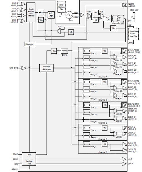
The 8V19N490-19BDGI is a fully integrated FemtoClock® NG jitter attenuator and clock synthesizer, a high-performance clock solution for conditioning and frequency/phase management of radio equipment boards in wireless base stations. The 8V19N490-19BDGI has been optimized to offer outstanding phase noise performance, meeting the requirements of GSM, WCDMA, LTE and LTE-A radio board implementations. This device supports JESD204B subclass 0 and 1 clocks.
The two-level PLL architecture supports jitter attenuation and frequency doubling. The first-level PLL is a jitter attenuator, which uses an external VCXO to achieve the best phase noise characteristics. The second-level PLL locks the VCXO-PLL output signal and synthesizes the target frequency.
The 8V19N490-19BDGI supports generating high-frequency clocks from the selected VCO and low-frequency synchronization signals (SYSREF). The SYSREF signal is internally synchronized with the clock signal. In addition, it also has a delay function, which can adjust and control the phase delay between the system reference signal and the clock signal, and can adjust/delay individual output signals. Monitor the activities of the four redundant input terminals. The 8V19N490-19BDGI offers four optional clock switching modes for handling clock input failure situations. The automatic locking, separately programmable output divider and phase adjustment functions have been added to enhance flexibility. The 8V19N490-19BDGI is configured via a three-wire SPI interface and reports the locked and signal loss status through internal registers and LOCK detection (LOCK) output. Internal status bit changes can also be reported through nINT output. The 8V19N490-19BDGI is an ideal choice for driver converter circuits in wireless infrastructure, radar/imaging, and instrument/medical applications.
Application scenarios
The 8V19N490-19BDGI is mainly used in scenarios with high requirements for clock accuracy, such as wireless base stations and communication equipment. It meets the demands of high-speed signal transmission by optimizing phase noise performance.
Consult Mingjiada immediately to get your exclusive supply plan
Official website: www.mjdic.com
Telephone: +86 13410018555 (Mr. Chen)
Email: sales@hkmjd.com