The official website - Shenzhen Mingjiada Electronic Co., LTD

-5V Inverting Negative Output Current Mode PWM Regulator ST ST735CD ST735
| Part number | Brand | Date | QTY | Package | Remarks |
| ST735CD | ST |
14+ROHS | 9900 | SOP-8 |
Original have in stock |
PDF datasheet:![]()
Specifications, Features, Applications
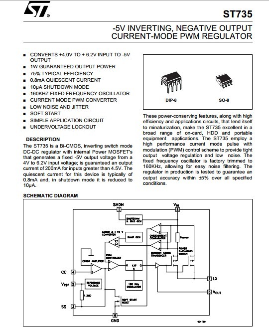
CONVERTS + 6.2V INPUT TO -5V OUTPUT 1W GUARANTEED OUTPUT POWER 75% TYPICAL EFFICIENCY 0.8mA QUIESCENT CURRENT 10µA SHUTDOWN MODE 160KHZ FIXED FREQUENCY OSCILLATOR CURRENT MODE PWM CONVERTER LOW NOISE AND JITTER SOFT START SIMPLE APPLICATION CIRCUIT UNDERVOLTAGE LOCKOUT
DESCRIPTION The is a Bi-CMOS, inverting switch mode DC-DC regulator with internal Power MOSFET's that generates a fixed -5V output voltage from to 6.2V input voltage; is guaranteed an output current of 200mA for inputs greater than 4.5V. The quiescent current for this device is typically of 0.8mA and, in shutdown mode it is reduced to 10µA. SCHEMATIC DIAGRAM
These power-conserving features, along with high efficiency and applications circuits, that lend itself to minaturization, make the ST735 excellent in a broad range of on-card, HDD and portable equipment applications. The ST735 employ a high performance current mode pulse with modulation (PWM) control scheme to provide tight output voltage regulation and low noise. The fixed frequency oscillator is factory trimmed to 160KHz, allowing for easy noise filtering. The regulator in production is tested to guarantee an output accuracy within ±5% over all specified conditions.
Symbol VIN SHDN VLX VFB VOUT ILX Ptot Tstg Top Parameter DC Input Voltage (VIN to GND) Shutdown Voltage (SHDN to GND) Switch Voltage (Lx to VIN) Feedback Voltage (VOUT to GND) Output Voltage (VOUT to GND) Other Input Voltage (SS, CC to GND) Peack Switch Current Power Dissipation = 70°C Storage Temperature Range Operating Junction Temperature Range DIP-8 SO-8 Value to +125 Unit mW °C
Absolute Maximum Ratings are those values beyond which damage to the device may occur. Functional operation under these condition is not implied.
Symbol Rthj-case Parameter Thermal Resistance Junction-case SO-8 8 Unit °C/W
Pin N° Symbol SHDN VREF SS CC VOUT GND LX VIN Reference Output Voltage Soft Start Compensation Input Negative Output Voltage Ground Switch Output Positive Supply - Voltage Input Name and Function SHUT-DOWN Control (VCC=ON GND=Shutdown
NOTE: 1) All capacitors are X7R ceramic 2) C5 can be omitted if are used higher values for the input and output capacitors C2=47µF, C1=100pF.
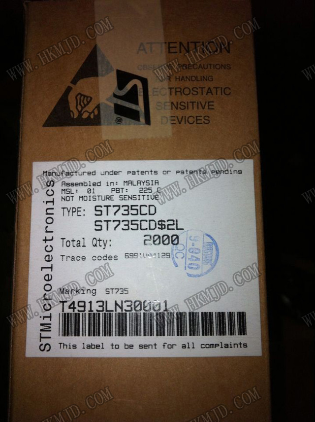
PHOTO:
Shenzhen Mingjiada Electronics Co., Ltd.
------------------------------------------------------------------
1239-1241 NEW ASIA GUOLI BUILDING
ZHENZHONG ROAD,FUTIAN DISTRICT,
SHENZHEN,CHINA 518031
Tel:+86-755-83957301ext.605
Fax:+86-755-83957753
Skype:mjdccm898
MSN: mingjiada8@hotmail.com
Yahoo: mjdccm898@yahoo.cn
Web:www.hkmjd.com
www.szmjd.en.alibaba.com
Email:sales@hkmjd.com